 RapidRTL
What synthesis does to Verilog, pass by pass
Synthesis turns HDL into a netlist: a graph whose nodes are cells, such as adders, multiplexers and flip-flops, and whose edges are the wires between them. A synthesis tool builds this graph from the code, then rewrites it in a series of passes until every cell is a primitive the target device provides. The graph between passes is the tool’s intermediate representation (IR).
This page follows a 4-bit counter through each pass of Yosys, an open-source synthesis tool that can write its IR, called RTLIL, as text after any pass, and compares the result with Vivado’s elaborated and synthesized designs.
The counter
module counter (
  input  wire       clk,
  input  wire       rst,
  input  wire       en,
  output reg  [3:0] count
);
  always @(posedge clk) begin
    if (rst)
      count <= 4'd0;
    else if (en)
      count <= count + 4'd1;
  end
endmodule
On each rising edge of clk, count is cleared when rst is high and
increases by one when en is high.
The passes
| Step | Pass | What changes | Cells |
|---|---|---|---|
| 1 | read_verilog | The text becomes a syntax tree, then RTLIL. The always block is kept as a process. | 1, and a process |
| 2 | proc | The process becomes multiplexers and a flip-flop. | 4 |
| 3 | opt | The reset and the enable are folded into the flip-flop. | 2 |
| 4 | techmap | Every cell becomes one-bit gates. | 47 |
| 5 | synth_xilinx | The logic is minimised and mapped to Xilinx 7-series primitives. | 6 |
1. Parsing: the syntax tree and the process
The parser first reads the text into a syntax tree. Each construct in the code is a node, and the parts it is made of are its children: an assignment has the signal it writes and the expression it writes, an addition has its two operands. Names and numbers are the leaves.
The tree is then converted to RTLIL. An expression becomes a cell at once:
the AST_ADD node is an $add cell. The always block is not converted to
hardware yet. It is stored as a process: the decision tree of the if
statements as switch rules, and a sync rule that says when the result is
stored.
process $proc$counter.v:7$1
  assign $0\count[3:0] \count
  switch \rst
    case 1'1
      assign $0\count[3:0] 4'0000
    case
      switch \en
        case 1'1
          assign $0\count[3:0] $add$counter.v:11$2_Y
        case
      end
  end
  sync posedge \clk
    update \count $0\count[3:0]
end
$0\count[3:0] is the value count will take. It starts as count, becomes
0 when rst is 1, becomes the adder’s output when en is 1, and is stored
in count on the rising edge of clk. A process has no schematic, because
it describes behaviour rather than cells.
2. proc: from process to cells
proc converts each process into cells. Each switch becomes a multiplexer
and the sync rule becomes a flip-flop.
- Adder.
count + 1. - Enable. Passes the adder's output when
enis 1, andcountwhen it is 0. - Reset. Passes
0whenrstis 1. - Register. A 4-bit flip-flop (
$dff) clocked byclk.
Each cell keeps a src attribute: the lines and columns of the code it came
from. The reset multiplexer in RTLIL:
attribute \src "counter.v:8.9-8.12|counter.v:8.5-11.29"
cell $mux $procmux$6
  parameter \WIDTH 4
  connect \A $procmux$3_Y
  connect \B 4'0000
  connect \S \rst
  connect \Y $0\count[3:0]
end
A is selected when S is 0 and B when S is 1. Latches are created in
this pass: in a combinational process, a path through the decision tree that
assigns nothing becomes a $dlatch. See
inferred latches in Verilog.
This is the As-Written view in the RapidRTL web editor.
3. opt: optimisation
opt runs a set of passes that fold constants, remove unused cells and merge
identical ones. On this design the pass that acts is opt_dff. A multiplexer
in front of a flip-flop that selects a constant when a signal is high is a
synchronous reset. A multiplexer that selects the flip-flop’s own output is an
enable. Both are folded into the flip-flop.
- Register with reset and enable.
$sdffe: a flip-flop with a synchronous reset (SRST) and an enable (EN). - Adder. Unchanged.
cell $sdffe $auto$ff.cc:337:slice$10
  parameter \SRST_VALUE 4'0000
  parameter \WIDTH 4
  connect \CLK \clk
  connect \EN \en
  connect \SRST \rst
  connect \D $add$counter.v:11$2_Y
  connect \Q \count
end
The folded form matches the device: an FPGA flip-flop has its own clock-enable and reset pins, so the reset and the enable cost no logic. This is the High-Level view.
4. techmap: generic gates
techmap replaces each multi-bit cell with one-bit gates from Yosys’s
internal library: $_AND_, $_OR_, $_XOR_, $_NOT_, $_MUX_ and
$_DFF_P_. In this view the reset and the enable are first split out of the
register again, so every cell is a basic gate.
| Came from | Gates |
|---|---|
| the adder | 12 $_XOR_, 9 $_AND_, 6 $_OR_, 4 $_NOT_, 4 $_MUX_ |
| the reset and the enable | 8 $_MUX_ |
| the register | 4 $_DFF_P_ |
The adder is a general 4-bit adder: one input is still the constant 1, and it keeps the logic that would invert an input for a subtraction. Nothing has been simplified yet. This is the Gate-Level view.
5. Mapping to the device
An FPGA builds logic from two kinds of block. A LUT (look-up table) is a small memory holding the truth table of any function of up to six inputs on 7-series devices. A carry chain is dedicated logic that passes the carry of an addition from bit to bit, faster than LUTs could.
synth_xilinx runs the full flow for Xilinx 7-series: passes like the ones
above, then abc, which minimises the logic and maps it to LUTs, and passes
that map flip-flops and carry chains to the device’s primitives.
- Register. Four
FDREflip-flops, one per bit, withenonCEandrstonR: the$sdffefrom step 3. - Inverter. Bit 0 of
count, inverted. - Adder. One
CARRY4: four bits of carry chain.
Adding 1 to a binary number inverts bit 0, and inverts every higher bit whose
lower bits are all 1. With c = count and n = count + 1:
The AND of the lower bits is the carry into bit i. The CARRY4 computes
it: its S inputs are count[3:1] and the inverted bit 0, and each output
bit is S XOR the carry into that bit. The 47 gates of step 4 become 6
primitives.
RapidRTL draws this mapping when an FPGA family is set as the target (free in the web editor, part of Pro in the VS Code extension).
Comparison with Vivado
The same file synthesized with Vivado 2025.1 for an Artix-7 (xc7a35t).
Elaborated design
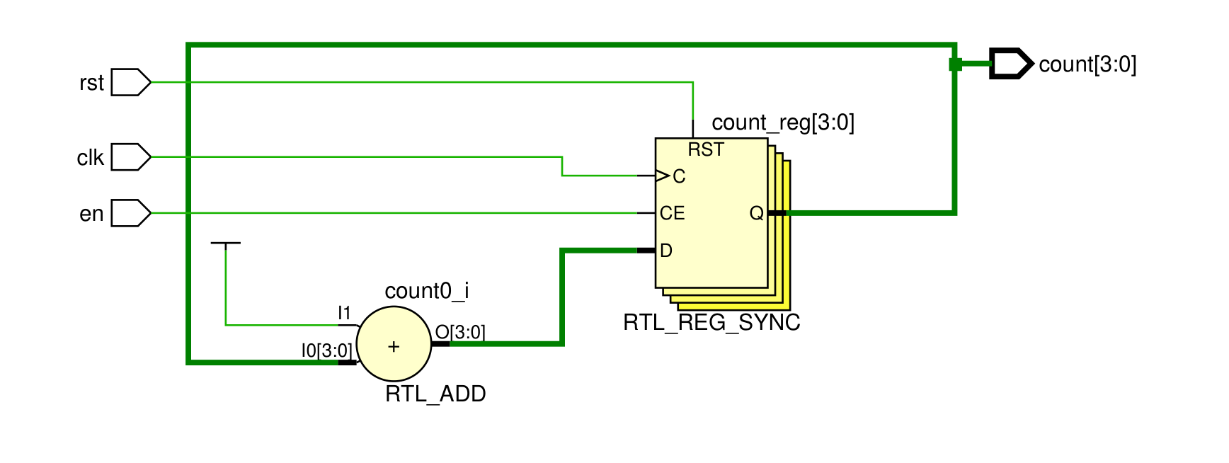
RTL_ADD) and one 4-bit register (RTL_REG_SYNC), drawn as a stack.The register has en on CE and rst on RST, and the constant 1 is the
tie-high on the adder’s I1 input. There are no multiplexers: Vivado
recognises the reset and the enable during elaboration, so its elaborated
design corresponds to step 3, not step 2.
Synthesized design
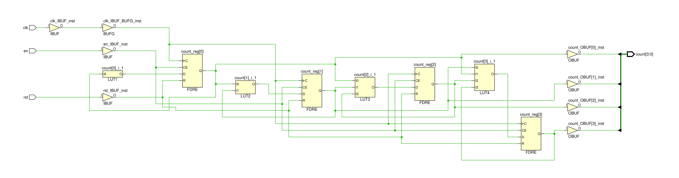
FDRE, one each of LUT1 to LUT4, and the pin buffers. Click it for the full-size image.| Primitive | Yosys | Vivado | Function |
|---|---|---|---|
FDRE | 4 | 4 | the register, en on CE and rst on R |
CARRY4 | 1 | 0 | count + 1 on the carry chain |
INV | 1 | 0 | bit 0 of count + 1 |
LUT1 to LUT4 | 0 | 4 | count + 1, one LUT per bit |
IBUF, OBUF, BUFG | not drawn | 3, 4, 1 | a buffer on every pin and on the clock |
The register is the same in both netlists. The adder is not: Vivado puts each
bit of the equation above in its own LUT. Bit i depends on i + 1 bits of
count, so bit 0 is a LUT1, bit 1 a LUT2, and bit 3 a LUT4. Their
INIT values are the truth tables: LUT2 has INIT = 6, binary 0110,
which is XOR. Vivado packs these four into two physical LUTs, each with two
outputs, so its utilisation report counts 2 LUTs. Both netlists compute the
same function.
The same stages in other tools
Every synthesis tool works on a netlist graph and refines it in steps. The tools differ in which steps they show.
| Tool | Generic netlist | Mapped netlist |
|---|---|---|
| Yosys | RTLIL after any pass (write_rtlil) | device primitives, after synth_xilinx, synth_ice40 and others |
| Vivado | elaborated design (RTL_ADD, RTL_MUX, RTL_REG) | synthesized design (LUT, FDRE, CARRY4) |
| Quartus | RTL Viewer, after Analysis & Elaboration | Technology Map Viewer, after mapping and after fitting |
| Design Compiler (ASIC) | GTECH generic gates | cells of the target standard-cell library |
Yosys writes its whole IR as text after any pass. Vivado and Quartus show
their netlists as schematics at fixed points, and Vivado’s Tcl console can
query them with get_cells and get_nets. Their internal formats are not
published.
Synthesis ends with mapped primitives. Place and route then assigns each primitive a location on the device and each net a path through the routing. In Vivado this is implementation. For Yosys netlists, nextpnr does it for several FPGA families.
Next steps
- Latches. An
always @(*)block that leaves an output unassigned on one path becomes a$dlatchin step 2. See latches in Verilog. - State machines. Between steps 3 and 5, the
fsmpass finds state registers and can re-encode them. See FSM design. - Wider adders. See adder architectures for how carry chains scale.