 RapidRTL
An FIR filter in VHDL, from equation to FPGA
An FIR (finite impulse response) filter computes each output sample as a weighted sum of the M most recent input samples:
M is the number of taps and bk are the coefficients. In hardware the delayed samples are held in registers, each coefficient is a multiplier, and the sum is one or more adders.
This page implements the simplest case, a two-tap moving average, in VHDL, shows the circuit it synthesizes to, and compares RapidRTL’s schematic with Vivado’s.
The two-tap moving average
With M = 2 and both coefficients equal to ½:
Each output is the average of the current sample and the previous one. This is a low-pass filter with magnitude response , where ω is in radians per sample. A constant input passes unchanged. An input alternating between +A and −A, a tone at half the sample rate, is removed.
From equation to hardware
| Term | Hardware | Cost for 8-bit samples |
|---|---|---|
x[n-1] | a register, clocked once per sample | 8 flip-flops |
+ | an adder one bit wider than the samples, so the sum cannot overflow | one 9-bit adder |
/ 2 | a right shift by one bit | none |
A right shift by one bit divides a binary number by two, in the same way
that dropping the last digit of a decimal number divides it by ten. A shift
by a fixed amount needs no logic: y is wired to bits 8 down to 1 of the
sum, and bit 0 is left unconnected.
The VHDL
One 8-bit signed sample arrives on x every clock cycle.
library ieee;
use ieee.std_logic_1164.all;
use ieee.numeric_std.all;

-- Two-tap moving average: y[n] = (x[n] + x[n-1]) / 2
entity fir_avg2 is
  port (
    clk : in  std_logic;
    x   : in  signed(7 downto 0);    -- x[n], one sample per clock
    y   : out signed(7 downto 0)     -- y[n]
  );
end entity;

architecture rtl of fir_avg2 is
  signal x_prev : signed(7 downto 0) := (others => '0');   -- x[n-1]
  signal sum    : signed(8 downto 0);                      -- one bit wider
begin
  -- The delay: a register that hands back last cycle's sample.
  process (clk) is
  begin
    if rising_edge(clk) then
      x_prev <= x;
    end if;
  end process;

  -- The adder: widen both samples to 9 bits first, so the sum cannot overflow.
  sum <= resize(x, 9) + resize(x_prev, 9);

  -- The divide by two: leave out the lowest bit. No logic, only wiring.
  y <= sum(8 downto 1);
end architecture;signedports. The samples are two’s complement, so+andresizehandle negative values correctly. See VHDL data types.- 9-bit sum. Two 8-bit values can need 9 bits:
100 + 100 = 200, which is above the 8-bit signed maximum of 127 and would wrap to-56.resizesign-extends each sample to 9 bits before the addition. sum(8 downto 1). The right shift by one bit, written as a slice.
The divide by two
A right shift by one bit moves every bit to the position below it, where it
is worth half as much, so the value is halved. y <= sum(8 downto 1) is
that shift: bit 8 of sum drives bit 7 of y, bit 7 drives bit 6, and so
on. For 100 + 100:
Bit of sum | 8 | 7 | 6 | 5 | 4 | 3 | 2 | 1 | 0 |
|---|---|---|---|---|---|---|---|---|---|
Weight in sum | -256 | 128 | 64 | 32 | 16 | 8 | 4 | 2 | 1 |
sum = 200 | 0 | 1 | 1 | 0 | 0 | 1 | 0 | 0 | 0 |
Drives bit of y | 7 | 6 | 5 | 4 | 3 | 2 | 1 | 0 | none |
Weight in y | -128 | 64 | 32 | 16 | 8 | 4 | 2 | 1 | 0 |
The three set bits are worth 128 + 64 + 8 = 200 in sum and 64 + 32 + 4 =
100 in y. The top bit has a negative weight because the value is signed.
Bit 0 of the sum is unconnected, so the result rounds down: 5 gives 2 and -5
gives -3.
In the schematics below the divide is therefore not a component. It is the one output bit of the adder that is left unconnected.
The circuit
The schematic RapidRTL draws from that code, with each step boxed:
- Delay. The register, drawn with a clock triangle. Its output is
x_prev, thex[n-1]term. - Sign extension.
resize(x, 9). The first bar selects bit 7, the sign. The second joins it to bits0:7as bit8. Wiring only. - Adder. One 9-bit adder.
- Divide by two. The bar labelled
1:8passes bits 1 to 8 of the sum toy. Bit 0 stops there. Wiring only.
The same design as a live schematic, next to its code:
Interactive schematic by RapidRTL
Response
A step input: x is 0, then 100 for three samples, then 0.
In cycle 2 the input is 100 and the register still holds 0, so y is 50. In
cycle 3 both are 100. The edge in x becomes a ramp in y, which is the
low-pass behaviour seen in the time domain.
An input alternating between +50 and -50, a tone at half the sample rate:
The first output is 25 because the register starts at 0.
y changes in the same cycle as x: the only register is on the delay path,
so the output is combinational from the input. Registering y as well costs
8 more flip-flops and one cycle of latency.
Comparison with Vivado
The same file synthesized with Vivado 2025.1 for an Artix-7 (xc7a35t).
Elaborated design
The code as generic blocks, before it is mapped to the device.
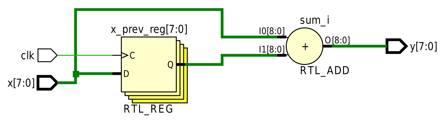
RTL_REG) and one adder (RTL_ADD).This is the same register and adder. Vivado draws each bus as one line and
does not draw the sign extension or the bit selection, so the divide by two
shows only in the widths: the adder’s output is O[8:0] and the port it
drives is y[7:0]. RapidRTL draws both, as the bars in boxes 2 and 4, which
shows that the dropped bit is bit 0.
Synthesized design
An FPGA builds an adder from look-up tables and a carry chain. RapidRTL shows this mapping when an FPGA family is set as the target (free in the web editor, part of Pro in the VS Code extension). For Xilinx 7-series:
- Delay. Eight
FDREflip-flops, one per bit ofx_prev. - Adder, first stage. Eight
LUT2cells, each the XOR of one bit ofxand the same bit ofx_prev. - Carry chain. Three
CARRY4cells, four bits each, chained from the top left to the bottom right. The first two produce bits 0 to 7 of the sum, the third bit 8. - Divide by two. The bar labelled
1:3on the output of the firstCARRY4passes bits 1 to 3 on, as bits 0 to 2 ofy. Bit 0 is unconnected.
Interactive schematic by RapidRTL
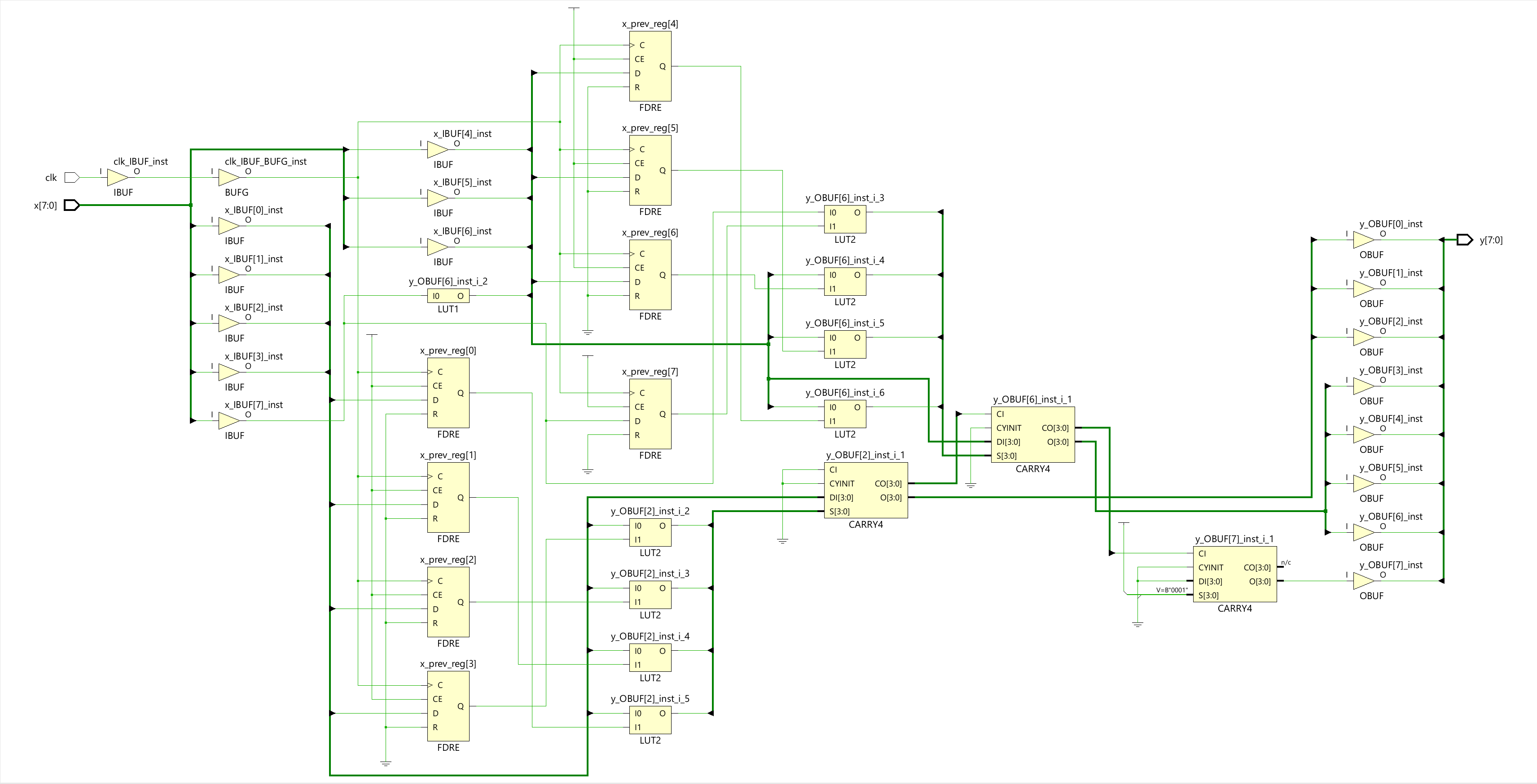
Vivado’s result for the same file:
| Primitive | RapidRTL | Vivado | Function |
|---|---|---|---|
FDRE | 8 | 8 | the register: one flip-flop per bit of x_prev |
LUT2 | 8 | 8 | the adder’s first stage: the XOR of each pair of input bits |
CARRY4 | 3 | 3 | the carry chain: four bits of the sum each |
LUT1 | 0 | 1 | an inverter on the sign bit of x |
IBUF, OBUF | not drawn | 9, 8 | a buffer on every pin |
BUFG | not drawn | 1 | the clock buffer |
Both schematics contain the same filter: 8 flip-flops for the delay, and 8
LUT2 cells feeding 3 CARRY4 cells for the 9-bit adder. The divide by two
is in neither column because it is not a primitive. In Vivado’s schematic it is in the same
place: the first CARRY4 (y_OBUF[2]_inst_i_1) has a four-bit output that
drives only three output buffers, y[0] to y[2].
The results differ in two places:
LUT1. Vivado adds an inverter on bit 7 ofx, the sign bit, where it enters the carry chain. Bit 8 of the sum is formed differently in the two schematics. In the boxed one, bit 7’s XOR is fed into the carry chain a second time. In Vivado’s, the sign bit is inverted going in and the last carry is inverted coming out. The sums are equal. Vivado’s utilisation report still counts 8 LUTs, because two of the nine share one physical LUT.- Pin buffers. Vivado synthesizes the file as a top-level design, so every
port gets an
IBUForOBUFand the clock aBUFG. RapidRTL draws only the logic.
Next steps
- Register the output. Move the assignment to
yinto the clocked process. A second register appears and the output is one cycle later. - More taps. A four-tap average needs three delays, three adders and
sum(9 downto 2). Each doubling of the length adds one bit to the sum. - General coefficients. Each tap is multiplied by its coefficient before the sum. See multipliers and adders.